Package Thermal Characterization
Introduction
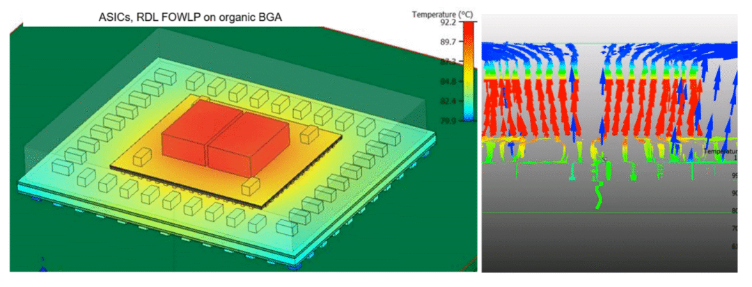
Effective heat removal from the IC chip, through the package,to the adjacent environment is crucial to maintain an allowable device junction temperature. The latter directly affects the electrical circuit performance both at the component and system levels. Aside from thermal enhancement of individual packages by the IC manufacturers, proper printed circuit board (PCB) layout and cabinet design by the end users can also substantially reduce the overall package thermal resistance.
The fundamentals of various heat transfer modes can be found in any classic heat transfer textbook, and recent advances in heat transfer and fluid flow development can be referred from published technical papers. Thus, the intent of this application note is threefold:
1. provide practical aspects of package thermal resistance definition;
2. show how the data are generated; and,
3. discuss package mounting, board effect, and system effect on heat transfer.
This application note first covers the basics of package thermal characterization to help the end user in interpreting the package thermal data. Subsequently, the package mounting effects, board effects, and system effects on package heat transfer are outlined, along with some critical dimensions.
The last section is a summary of major guidelines for the end user to obtain a better thermal design at the board and system levels.
Package Thermal Characterization
-------------
Summary
A thermal resistance approach by electrical analogy, so far, is the simplest method for analyzing the thermal behavior from the component level up to the system level. The following practical thermal guidelines may be useful in providing component and system reliability, which meet the best interests nof both semiconductor manufacturers and end users:
1. Provide sufficient conduction paths from the package to the board or adapt a direct heat sink approach,
2. Enhance the convective heat transfer to the board or along the board in the cabinet by diverting flow to simulate jet impingement at the hot spot regions,
3. Place high power devices near the leading edge or trailing edge of the board when the board is oriented vertically.
On the other hand, when the board is oriented horizontally, position the high power devices face up within the center,
4. Mounting of any heat sink on a package should also take into consideration the heat transfer effect on adjacent packages,
5. Strengthen the radiant heat with an increase of surface emissivity.
The overall thermal resistance of a package can be reduced significantly by addressing the comprehensive thermal management from the component level, to the board level, and up to the system level.
References
1. P. C. Lin, “Thermal Characterization of SemiconductorPackages”, Nordic Cooling of Electronics Conference,Gothenberg, Sweden, November 18–19 (1992).
2. R. M. Mindock, “Thermal Resistances of Joint ArmyNavy (JAN) Certified Microcircuit Packages”,RADC-TR-86-97, Rome Air Development Center, AirForce Systems Command, Griffiss AFB, NY (1986).
3. R. Pendse and B. J. Shanker, “A Study of Thermal Performanceof Packages Using A New Test Die”, 4th IEEE
Semiconductor Thermal and Temperature MeasurementSymp., pp. 50–54 (1988).
4. C. Simpson, “The Fundamental of Thermal Design”,Electronic Design, pp. 95–100, September 26 (1991).
熱設(shè)計(jì)資料下載: PACKAGE_THERMAL_CHARACTERIZATION-MISC.pdf
標(biāo)簽: 點(diǎn)擊: 評論: